Пишем программу Blink и прошиваем микроконтроллер AT90S2013.
.include "2313def.inc"
.EQU pin=6
.org 0x00
            rjmp reset
            reti
            reti
            reti
            reti
            reti
            reti
            reti
            reti
            reti
            reti
.org 0x0b
reset:      sbi DDRD, pin
loop:       sbi PORTD, pin
            ldi r23, 1
            rcall delaytime

            cbi PORTD, pin
            ldi r23, 20
            rcall delaytime
            rjmp loop
delaytime:                      ; Задержка
            sbiw r25:r24,1
            sbci r23,0
            brcc delaytime
            ret
Лист. 1. Программа Blink для микроконтроллера AT90S2013.
Скомпилировать программу можно с помощью компилятора avra:
avra test.s
После компиляции файла test.s получим двоичный файл test.s.hex пригодный для загрузки в микроконтроллер.
avrdude -p2313 -cUSBASP -Uflash:w:test.s.hex:i -F
avrdude: warning at /home/dior/.avrduderc:56: part 8052 overwrites previous definition /home/dior/.avrduderc:5.

avrdude: warning: cannot set sck period. please check for usbasp firmware update.
avrdude: AVR device initialized and ready to accept instructions

Reading | ################################################## | 100% 0.00s

avrdude: Device signature = 0x1e9101 (probably 2313)
avrdude: NOTE: "flash" memory has been specified, an erase cycle will be performed
         To disable this feature, specify the -D option.
avrdude: erasing chip
avrdude: warning: cannot set sck period. please check for usbasp firmware update.
avrdude: reading input file "test.s.hex"
avrdude: writing flash (28 bytes):

Writing | ################################################## | 100% 0.14s

avrdude: 28 bytes of flash written
avrdude: verifying flash memory against test.s.hex:
avrdude: load data flash data from input file test.s.hex:
avrdude: input file test.s.hex contains 28 bytes
avrdude: reading on-chip flash data:

Reading | ################################################## | 100% 0.03s

avrdude: verifying ...
avrdude: 28 bytes of flash verified

avrdude: safemode: Sorry, reading back fuses was unreliable. I have given up and exited programming mode

avrdude done.  Thank you.
Shell
;***** THIS IS A MACHINE GENERATED FILE - DO NOT EDIT ********************
;***** Created: 2011-02-09 12:03 ******* Source: AT90S2313.xml ***********
;*************************************************************************
;* A P P L I C A T I O N N O T E F O R T H E A V R F A M I L Y
;*
;* Number : AVR000
;* File Name : "2313def.inc"
;* Title : Register/Bit Definitions for the AT90S2313
;* Date : 2011-02-09
;* Version : 2.35
;* Support E-mail : Адрес электронной почты защищен от спам-ботов. Для просмотра адреса в вашем браузере должен быть включен Javascript.
;* Target MCU : AT90S2313
;*
;* DESCRIPTION
;* When including this file in the assembly program file, all I/O register
;* names and I/O register bit names appearing in the data book can be used.
;* In addition, the six registers forming the three data pointers X, Y and
;* Z have been assigned names XL - ZH. Highest RAM address for Internal
;* SRAM is also defined
;*
;* The Register names are represented by their hexadecimal address.
;*
;* The Register Bit names are represented by their bit number (0-7).
;*
;* Please observe the difference in using the bit names with instructions
;* such as "sbr"/"cbr" (set/clear bit in register) and "sbrs"/"sbrc"
;* (skip if bit in register set/cleared). The following example illustrates
;* this:
;*
;* in r16,PORTB ;read PORTB latch
;* sbr r16,(1<<PB6)+(1<<PB5) ;set PB6 and PB5 (use masks, not bit#)
;* out PORTB,r16 ;output to PORTB
;*
;* in r16,TIFR ;read the Timer Interrupt Flag Register
;* sbrc r16,TOV0 ;test the overflow flag (use bit#)
;* rjmp TOV0_is_set ;jump if set
;* ... ;otherwise do something else
;*************************************************************************
#ifndef _2313DEF_INC_
#define _2313DEF_INC_
;#pragma partinc 0
; ***** SPECIFY DEVICE ***************************************************
.device AT90S2313
;#pragma AVRPART ADMIN PART_NAME AT90S2313
.equ SIGNATURE_000 = 0x1e
.equ SIGNATURE_001 = 0x91
.equ SIGNATURE_002 = 0x01
;#pragma AVRPART CORE CORE_VERSION V1
; ***** I/O REGISTER DEFINITIONS *****************************************
; NOTE:
; Definitions marked "MEMORY MAPPED"are extended I/O ports
; and cannot be used with IN/OUT instructions
.equ SREG = 0x3f
.equ SPL = 0x3d
.equ GIMSK = 0x3b
.equ GIFR = 0x3a
.equ TIMSK = 0x39
.equ TIFR = 0x38
.equ MCUCR = 0x35
.equ TCCR0 = 0x33
.equ TCNT0 = 0x32
.equ TCCR1A = 0x2f
.equ TCCR1B = 0x2e
.equ TCNT1L = 0x2c
.equ TCNT1H = 0x2d
.equ OCR1AL = 0x2a
.equ OCR1AH = 0x2b
.equ ICR1L = 0x24
.equ ICR1H = 0x25
.equ WDTCR = 0x21
.equ EEAR = 0x1e
.equ EEDR = 0x1d
.equ EECR = 0x1c
.equ PORTB = 0x18
.equ DDRB = 0x17
.equ PINB = 0x16
.equ PORTD = 0x12
.equ DDRD = 0x11
.equ PIND = 0x10
.equ UDR = 0x0c
.equ USR = 0x0b
.equ UCR = 0x0a
.equ UBRR = 0x09
.equ ACSR = 0x08
; ***** BIT DEFINITIONS **************************************************
; ***** PORTB ************************
; PORTB - Port B Data Register
.equ PORTB0 = 0 ; Port B Data Register bit 0
.equ PB0 = 0 ; For compatibility
.equ PORTB1 = 1 ; Port B Data Register bit 1
.equ PB1 = 1 ; For compatibility
.equ PORTB2 = 2 ; Port B Data Register bit 2
.equ PB2 = 2 ; For compatibility
.equ PORTB3 = 3 ; Port B Data Register bit 3
.equ PB3 = 3 ; For compatibility
.equ PORTB4 = 4 ; Port B Data Register bit 4
.equ PB4 = 4 ; For compatibility
.equ PORTB5 = 5 ; Port B Data Register bit 5
.equ PB5 = 5 ; For compatibility
.equ PORTB6 = 6 ; Port B Data Register bit 6
.equ PB6 = 6 ; For compatibility
.equ PORTB7 = 7 ; Port B Data Register bit 7
.equ PB7 = 7 ; For compatibility
; DDRB - Port B Data Direction Register
.equ DDB0 = 0 ; Port B Data Direction Register bit 0
.equ DDB1 = 1 ; Port B Data Direction Register bit 1
.equ DDB2 = 2 ; Port B Data Direction Register bit 2
.equ DDB3 = 3 ; Port B Data Direction Register bit 3
.equ DDB4 = 4 ; Port B Data Direction Register bit 4
.equ DDB5 = 5 ; Port B Data Direction Register bit 5
.equ DDB6 = 6 ; Port B Data Direction Register bit 6
.equ DDB7 = 7 ; Port B Data Direction Register bit 7
; PINB - Port B Input Pins
.equ PINB0 = 0 ; Port B Input Pins bit 0
.equ PINB1 = 1 ; Port B Input Pins bit 1
.equ PINB2 = 2 ; Port B Input Pins bit 2
.equ PINB3 = 3 ; Port B Input Pins bit 3
.equ PINB4 = 4 ; Port B Input Pins bit 4
.equ PINB5 = 5 ; Port B Input Pins bit 5
.equ PINB6 = 6 ; Port B Input Pins bit 6
.equ PINB7 = 7 ; Port B Input Pins bit 7
; ***** TIMER_COUNTER_0 **************
; TIMSK - Timer/Counter Interrupt Mask Register
.equ TOIE0 = 1 ; Timer/Counter0 Overflow Interrupt Enable
; TIFR - Timer/Counter Interrupt Flag register
.equ TOV0 = 1 ; Timer/Counter0 Overflow Flag
; TCCR0 - Timer/Counter0 Control Register
.equ CS00 = 0 ; Clock Select0 bit 0
.equ CS01 = 1 ; Clock Select0 bit 1
.equ CS02 = 2 ; Clock Select0 bit 2
; TCNT0 - Timer Counter 0
.equ TCNT00 = 0 ; Timer Counter 0 bit 0
.equ TCNT01 = 1 ; Timer Counter 0 bit 1
.equ TCNT02 = 2 ; Timer Counter 0 bit 2
.equ TCNT03 = 3 ; Timer Counter 0 bit 3
.equ TCNT04 = 4 ; Timer Counter 0 bit 4
.equ TCNT05 = 5 ; Timer Counter 0 bit 5
.equ TCNT06 = 6 ; Timer Counter 0 bit 6
.equ TCNT07 = 7 ; Timer Counter 0 bit 7
; ***** TIMER_COUNTER_1 **************
; TIMSK - Timer/Counter Interrupt Mask Register
.equ TICIE1 = 3 ; Timer/Counter1 Input Capture Interrupt Enable
.equ OCIE1A = 6 ; Timer/Counter1 Output CompareA Match Interrupt Enable
.equ TOIE1 = 7 ; Timer/Counter1 Overflow Interrupt Enable
; TIFR - Timer/Counter Interrupt Flag register
.equ ICF1 = 3 ; Input Capture Flag 1
.equ OCF1A = 6 ; Output Compare Flag 1A
.equ TOV1 = 7 ; Timer/Counter1 Overflow Flag
; TCCR1A - Timer/Counter1 Control Register A
.equ PWM10 = 0 ; Pulse Width Modulator Select Bit 0
.equ PWM11 = 1 ; Pulse Width Modulator Select Bit 1
.equ COM1A0 = 6 ; Comparet Ouput Mode 1A, bit 0
.equ COM1A1 = 7 ; Compare Output Mode 1A, bit 1
; TCCR1B - Timer/Counter1 Control Register B
.equ CS10 = 0 ; Clock Select bit 0
.equ CS11 = 1 ; Clock Select 1 bit 1
.equ CS12 = 2 ; Clock Select1 bit 2
.equ CTC1 = 3 ; Clear Timer/Counter1 on Compare Match
.equ ICES1 = 6 ; Input Capture 1 Edge Select
.equ ICNC1 = 7 ; Input Capture 1 Noise Canceler
; ***** WATCHDOG *********************
; WDTCR - Watchdog Timer Control Register
.equ WDP0 = 0 ; Watch Dog Timer Prescaler bit 0
.equ WDP1 = 1 ; Watch Dog Timer Prescaler bit 1
.equ WDP2 = 2 ; Watch Dog Timer Prescaler bit 2
.equ WDE = 3 ; Watch Dog Enable
.equ WDTOE = 4 ; RW
.equ WDDE = WDTOE ; For compatibility
; ***** EXTERNAL_INTERRUPT ***********
; GIMSK - General Interrupt Mask Register
.equ INT0 = 6 ; External Interrupt Request 0 Enable
.equ INT1 = 7 ; External Interrupt Request 1 Enable
; GIFR - General Interrupt Flag register
.equ INTF0 = 6 ; External Interrupt Flag 0
.equ INTF1 = 7 ; External Interrupt Flag 1
; ***** UART *************************
; UDR - UART I/O Data Register
.equ UDR0 = 0 ; UART I/O Data Register bit 0
.equ UDR1 = 1 ; UART I/O Data Register bit 1
.equ UDR2 = 2 ; UART I/O Data Register bit 2
.equ UDR3 = 3 ; UART I/O Data Register bit 3
.equ UDR4 = 4 ; UART I/O Data Register bit 4
.equ UDR5 = 5 ; UART I/O Data Register bit 5
.equ UDR6 = 6 ; UART I/O Data Register bit 6
.equ UDR7 = 7 ; UART I/O Data Register bit 7
; USR - UART Status Register
.equ DOR = 3 ; Data overRun
.equ FE = 4 ; Framing Error
.equ UDRE = 5 ; UART Data Register Empty
.equ TXC = 6 ; UART Transmit Complete
.equ RXC = 7 ; UART Receive Complete
; UCR - UART Control Register
.equ TXB8 = 0 ; Transmit Data Bit 8
.equ RXB8 = 1 ; Receive Data Bit 8
.equ CHR9 = 2 ; 9-bit Characters
.equ TXEN = 3 ; Transmitter Enable
.equ RXEN = 4 ; Receiver Enable
.equ UDRIE = 5 ; UART Data Register Empty Interrupt Enable
.equ TXCIE = 6 ; TX Complete Interrupt Enable
.equ RXCIE = 7 ; RX Complete Interrupt Enable
; UBRR - UART BAUD Rate Register
.equ UBRR0 = 0 ; UART Baud Rate Register bit 0
.equ UBRR1 = 1 ; UART Baud Rate Register bit 1
.equ UBRR2 = 2 ; UART Baud Rate Register bit 2
.equ UBRR3 = 3 ; UART Baud Rate Register bit 3
.equ UBRR4 = 4 ; UART Baud Rate Register bit 4
.equ UBRR5 = 5 ; UART Baud Rate Register bit 5
.equ UBRR6 = 6 ; UART Baud Rate Register bit 6
.equ UBRR7 = 7 ; UART Baud Rate Register bit 7
; ***** ANALOG_COMPARATOR ************
; ACSR - Analog Comparator Control And Status Register
.equ ACIS0 = 0 ; Analog Comparator Interrupt Mode Select bit 0
.equ ACIS1 = 1 ; Analog Comparator Interrupt Mode Select bit 1
.equ ACIC = 2 ; Analog Comparator Input Capture Enable
.equ ACIE = 3 ; Analog Comparator Interrupt Enable
.equ ACI = 4 ; Analog Comparator Interrupt Flag
.equ ACO = 5 ; Analog Comparator Output
.equ ACD = 7 ; Analog Comparator Disable
; ***** CPU **************************
; SREG - Status Register
.equ SREG_C = 0 ; Carry Flag
.equ SREG_Z = 1 ; Zero Flag
.equ SREG_N = 2 ; Negative Flag
.equ SREG_V = 3 ; Two's Complement Overflow Flag
.equ SREG_S = 4 ; Sign Bit
.equ SREG_H = 5 ; Half Carry Flag
.equ SREG_T = 6 ; Bit Copy Storage
.equ SREG_I = 7 ; Global Interrupt Enable
; SPL - Stack Pointer Low
.equ SP0 = 0 ; Stack pointer bit 0
.equ SP1 = 1 ; Stack pointer bit 1
.equ SP2 = 2 ; Stack pointer bit 2
.equ SP3 = 3 ; Stack pointer bit 3
.equ SP4 = 4 ; Stack pointer bit 4
.equ SP5 = 5 ; Stack pointer bit 5
.equ SP6 = 6 ; Stack pointer bit 6
.equ SP7 = 7 ; Stack pointer bit 7
; MCUCR - MCU Control Register
.equ ISC00 = 0 ; Interrupt Sense Control 0 bit 0
.equ ISC01 = 1 ; Interrupt Sense Control 0 bit 1
.equ ISC10 = 2 ; Interrupt Sense Control 1 bit 0
.equ ISC11 = 3 ; Interrupt Sense Control 1 bit 1
.equ SM = 4 ; Sleep Mode
.equ SE = 5 ; Sleep Enable
; ***** PORTD ************************
; PORTD - Data Register, Port D
.equ PORTD0 = 0 ;
.equ PD0 = 0 ; For compatibility
.equ PORTD1 = 1 ;
.equ PD1 = 1 ; For compatibility
.equ PORTD2 = 2 ;
.equ PD2 = 2 ; For compatibility
.equ PORTD3 = 3 ;
.equ PD3 = 3 ; For compatibility
.equ PORTD4 = 4 ;
.equ PD4 = 4 ; For compatibility
.equ PORTD5 = 5 ;
.equ PD5 = 5 ; For compatibility
.equ PORTD6 = 6 ;
.equ PD6 = 6 ; For compatibility
; DDRD - Data Direction Register, Port D
.equ DDD0 = 0 ;
.equ DDD1 = 1 ;
.equ DDD2 = 2 ;
.equ DDD3 = 3 ;
.equ DDD4 = 4 ;
.equ DDD5 = 5 ;
.equ DDD6 = 6 ;
; PIND - Input Pins, Port D
.equ PIND0 = 0 ;
.equ PIND1 = 1 ;
.equ PIND2 = 2 ;
.equ PIND3 = 3 ;
.equ PIND4 = 4 ;
.equ PIND5 = 5 ;
.equ PIND6 = 6 ;
; ***** EEPROM ***********************
; EEAR - EEPROM Read/Write Access
.equ EEARL = EEAR ; For compatibility
.equ EEAR0 = 0 ; EEPROM Read/Write Access bit 0
.equ EEAR1 = 1 ; EEPROM Read/Write Access bit 1
.equ EEAR2 = 2 ; EEPROM Read/Write Access bit 2
.equ EEAR3 = 3 ; EEPROM Read/Write Access bit 3
.equ EEAR4 = 4 ; EEPROM Read/Write Access bit 4
.equ EEAR5 = 5 ; EEPROM Read/Write Access bit 5
.equ EEAR6 = 6 ; EEPROM Read/Write Access bit 6
; EEDR - EEPROM Data Register
.equ EEDR0 = 0 ; EEPROM Data Register bit 0
.equ EEDR1 = 1 ; EEPROM Data Register bit 1
.equ EEDR2 = 2 ; EEPROM Data Register bit 2
.equ EEDR3 = 3 ; EEPROM Data Register bit 3
.equ EEDR4 = 4 ; EEPROM Data Register bit 4
.equ EEDR5 = 5 ; EEPROM Data Register bit 5
.equ EEDR6 = 6 ; EEPROM Data Register bit 6
.equ EEDR7 = 7 ; EEPROM Data Register bit 7
; EECR - EEPROM Control Register
.equ EERE = 0 ; EEPROM Read Enable
.equ EEWE = 1 ; EEPROM Write Enable
.equ EEMWE = 2 ; EEPROM Master Write Enable
; ***** LOCKSBITS ********************************************************
.equ LB1 = 0 ; Lockbit
.equ LB2 = 1 ; Lockbit
; ***** FUSES ************************************************************
; LOW fuse bits
; ***** CPU REGISTER DEFINITIONS *****************************************
.def XH = r27
.def XL = r26
.def YH = r29
.def YL = r28
.def ZH = r31
.def ZL = r30
; ***** DATA MEMORY DECLARATIONS *****************************************
.equ FLASHEND = 0x03ff ; Note: Word address
.equ IOEND = 0x003f
.equ SRAM_START = 0x0060
.equ SRAM_SIZE = 128
.equ RAMEND = 0x00df
.equ XRAMEND = 0x0000
.equ E2END = 0x007f
.equ EEPROMEND = 0x007f
.equ EEADRBITS = 7
;#pragma AVRPART MEMORY PROG_FLASH 2048
;#pragma AVRPART MEMORY EEPROM 128
;#pragma AVRPART MEMORY INT_SRAM SIZE 128
;#pragma AVRPART MEMORY INT_SRAM START_ADDR 0x60
; ***** INTERRUPT VECTORS ************************************************
.equ INT0addr = 0x0001 ; External Interrupt Request 0
.equ INT1addr = 0x0002 ; External Interrupt Request 1
.equ ICP1addr = 0x0003 ; Timer/Counter1 Capture Event
.equ OC1addr = 0x0004 ; Timer/Counter1 Compare Match
.equ OVF1addr = 0x0005 ; Timer/Counter1 Overflow
.equ OVF0addr = 0x0006 ; Timer/Counter0 Overflow
.equ URXCaddr = 0x0007 ; UART, Rx Complete
.equ UDREaddr = 0x0008 ; UART Data Register Empty
.equ UTXCaddr = 0x0009 ; UART, Tx Complete
.equ ACIaddr = 0x000a ; Analog Comparator
.equ INT_VECTORS_SIZE = 11 ; size in words
;#pragma AVRPART CORE INSTRUCTIONS_NOT_SUPPORTED break
#endif /* _2313DEF_INC_ */
; ***** END OF FILE ******************************************************Лист. 2. Включаемый файл 2313def.inc
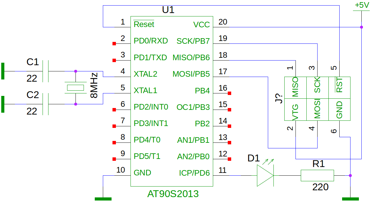
Рис. 1. Принципиальная электрическая схема подключения микроконтроллера к программатору.
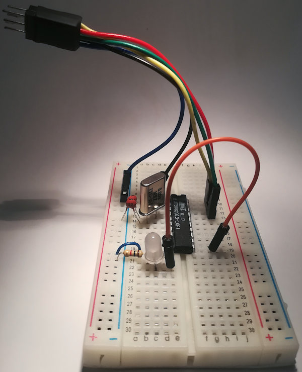
Рис. 2. Макет схемы для программирования микроконтроллера AT90S2313