Пишем программу Blink и прошиваем микроконтроллер ATtiny861.
Прежде чем программировать микроконтроллер установим фьюзы:
avrdude -pt861 -cusbasp -Uhfuse:w:0xdf:m -Ulfuse:w:0xe2:m

avrdude: warning: cannot set sck period. please check for usbasp firmware update.
avrdude: AVR device initialized and ready to accept instructions

Reading | ################################################## | 100% 0.00s

avrdude: Device signature = 0x1e930d (probably t861)
avrdude: reading input file "0xdf"
avrdude: writing hfuse (1 bytes):

Writing | ################################################## | 100% 0.00s

avrdude: 1 bytes of hfuse written
avrdude: verifying hfuse memory against 0xdf:
avrdude: load data hfuse data from input file 0xdf:
avrdude: input file 0xdf contains 1 bytes
avrdude: reading on-chip hfuse data:

Reading | ################################################## | 100% 0.00s

avrdude: verifying ...
avrdude: 1 bytes of hfuse verified
avrdude: reading input file "0xe2"
avrdude: writing lfuse (1 bytes):

Writing | ################################################## | 100% 0.00s

avrdude: 1 bytes of lfuse written
avrdude: verifying lfuse memory against 0xe2:
avrdude: load data lfuse data from input file 0xe2:
avrdude: input file 0xe2 contains 1 bytes
avrdude: reading on-chip lfuse data:

Reading | ################################################## | 100% 0.00s

avrdude: verifying ...
avrdude: 1 bytes of lfuse verified

avrdude: safemode: Fuses OK (E:FF, H:DF, L:E2)

avrdude done.  Thank you.
Shell 1.
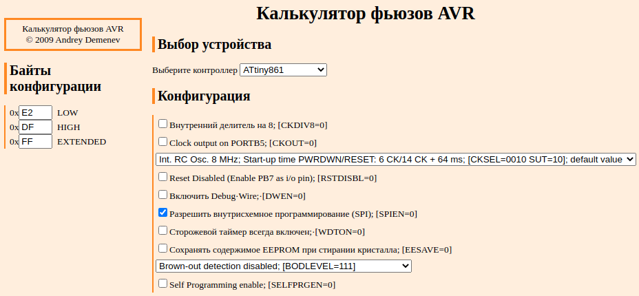
Рис. Калькулятор фьюзов с сайта http://homes-smart.ru/fusecalc/
.include "tn861Adef.inc"

.EQU pin=6
            sbi DDRB, pin

loop:       sbi PORTB, pin
            ldi r23, 1
            rcall delaytime

            cbi PORTB, pin
            ldi r23, 20
            rcall delaytime
            rjmp loop

delaytime:                      ; Задержка
            sbiw r25:r24,1
            sbci r23,0
            brcc delaytime
            ret
Лист. 1. Программа Blink для микроконтроллера ATtiny861.
Скомпилировать программу можно с помощью компилятора avra:
avra test.s
AVRA: advanced AVR macro assembler (version 1.4.2)
Pass 1...
Pass 2...
done


Assembly complete with no errors.
Segment usage:
   Code      :        12 words (24 bytes)
   Data      :         0 bytes
   EEPROM    :         0 bytes
Shell 1.
После компиляции файла test.s получим двоичный файл test.s.hex пригодный для загрузки в микроконтроллер.
avrdude -pt861 -cUSBASP -Uflash:w:test.s.hex:i

avrdude: warning: cannot set sck period. please check for usbasp firmware update.
avrdude: AVR device initialized and ready to accept instructions

Reading | ################################################## | 100% 0.00s

avrdude: Device signature = 0x1e930d (probably t861)
avrdude: NOTE: "flash" memory has been specified, an erase cycle will be performed
         To disable this feature, specify the -D option.
avrdude: erasing chip
avrdude: warning: cannot set sck period. please check for usbasp firmware update.
avrdude: reading input file "test.s.hex"
avrdude: writing flash (24 bytes):

Writing | ################################################## | 100% 0.03s

avrdude: 24 bytes of flash written
avrdude: verifying flash memory against test.s.hex:
avrdude: load data flash data from input file test.s.hex:
avrdude: input file test.s.hex contains 24 bytes
avrdude: reading on-chip flash data:

Reading | ################################################## | 100% 0.02s

avrdude: verifying ...
avrdude: 24 bytes of flash verified

avrdude: safemode: Fuses OK (E:FF, H:DF, L:E2)

avrdude done.  Thank you.
Shell
;***** THIS IS A MACHINE GENERATED FILE - DO NOT EDIT ********************
;***** Created: 2011-02-09 12:04 ******* Source: ATtiny861A.xml **********
;*************************************************************************
;* A P P L I C A T I O N   N O T E   F O R   T H E   A V R   F A M I L Y
;*
;* Number            : AVR000
;* File Name         : "tn861Adef.inc"
;* Title             : Register/Bit Definitions for the ATtiny861A
;* Date              : 2011-02-09
;* Version           : 2.35
;* Support E-mail    : avrСОБАКАatmel.com
;* Target MCU        : ATtiny861A
;*
;* DESCRIPTION
;* When including this file in the assembly program file, all I/O register
;* names and I/O register bit names appearing in the data book can be used.
;* In addition, the six registers forming the three data pointers X, Y and
;* Z have been assigned names XL - ZH. Highest RAM address for Internal
;* SRAM is also defined
;*
;* The Register names are represented by their hexadecimal address.
;*
;* The Register Bit names are represented by their bit number (0-7).
;*
;* Please observe the difference in using the bit names with instructions
;* such as "sbr"/"cbr" (set/clear bit in register) and "sbrs"/"sbrc"
;* (skip if bit in register set/cleared). The following example illustrates
;* this:
;*
;* in    r16,PORTB             ;read PORTB latch
;* sbr   r16,(1<<PB6)+(1<<PB5) ;set PB6 and PB5 (use masks, not bit#)
;* out   PORTB,r16             ;output to PORTB
;*
;* in    r16,TIFR              ;read the Timer Interrupt Flag Register
;* sbrc  r16,TOV0              ;test the overflow flag (use bit#)
;* rjmp  TOV0_is_set           ;jump if set
;* ...                         ;otherwise do something else
;*************************************************************************

#ifndef _TN861ADEF_INC_
#define _TN861ADEF_INC_


;#pragma partinc 0

; ***** SPECIFY DEVICE ***************************************************
.device ATtiny861A
;#pragma AVRPART ADMIN PART_NAME ATtiny861A
.equ	SIGNATURE_000	= 0x1e
.equ	SIGNATURE_001	= 0x93
.equ	SIGNATURE_002	= 0x0d

;#pragma AVRPART CORE CORE_VERSION V2
;#pragma AVRPART CORE NEW_INSTRUCTIONS lpm rd,z+


; ***** I/O REGISTER DEFINITIONS *****************************************
; NOTE:
; Definitions marked "MEMORY MAPPED"are extended I/O ports
; and cannot be used with IN/OUT instructions
.equ	SREG	= 0x3f
.equ	SPL	= 0x3d
.equ	SPH	= 0x3e
.equ	GIMSK	= 0x3b
.equ	GIFR	= 0x3a
.equ	TIMSK	= 0x39
.equ	TIFR	= 0x38
.equ	SPMCSR	= 0x37
.equ	PRR	= 0x36
.equ	MCUCR	= 0x35
.equ	MCUSR	= 0x34
.equ	TCCR0B	= 0x33
.equ	TCNT0L	= 0x32
.equ	OSCCAL	= 0x31
.equ	TCCR1A	= 0x30
.equ	TCCR1B	= 0x2f
.equ	TCNT1	= 0x2e
.equ	OCR1A	= 0x2d
.equ	OCR1B	= 0x2c
.equ	OCR1C	= 0x2b
.equ	OCR1D	= 0x2a
.equ	PLLCSR	= 0x29
.equ	CLKPR	= 0x28
.equ	TCCR1C	= 0x27
.equ	TCCR1D	= 0x26
.equ	TC1H	= 0x25
.equ	DT1	= 0x24
.equ	PCMSK0	= 0x23
.equ	PCMSK1	= 0x22
.equ	WDTCR	= 0x21
.equ	DWDR	= 0x20
.equ	EEARH	= 0x1f
.equ	EEARL	= 0x1e
.equ	EEDR	= 0x1d
.equ	EECR	= 0x1c
.equ	PORTA	= 0x1b
.equ	DDRA	= 0x1a
.equ	PINA	= 0x19
.equ	PORTB	= 0x18
.equ	DDRB	= 0x17
.equ	PINB	= 0x16
.equ	TCCR0A	= 0x15
.equ	TCNT0H	= 0x14
.equ	OCR0A	= 0x13
.equ	OCR0B	= 0x12
.equ	USIPP	= 0x11
.equ	USIBR	= 0x10
.equ	USIDR	= 0x0f
.equ	USISR	= 0x0e
.equ	USICR	= 0x0d
.equ	GPIOR2	= 0x0c
.equ	GPIOR1	= 0x0b
.equ	GPIOR0	= 0x0a
.equ	ACSRB	= 0x09
.equ	ACSRA	= 0x08
.equ	ADMUX	= 0x07
.equ	ADCSRA	= 0x06
.equ	ADCH	= 0x05
.equ	ADCL	= 0x04
.equ	ADCSRB	= 0x03
.equ	DIDR1	= 0x02
.equ	DIDR0	= 0x01
.equ	TCCR1E	= 0x00


; ***** BIT DEFINITIONS **************************************************

; ***** PORTA ************************
; PORTA - Port A Data Register
.equ	PORTA0	= 0	; Port A Data Register bit 0
.equ	PA0	= 0	; For compatibility
.equ	PORTA1	= 1	; Port A Data Register bit 1
.equ	PA1	= 1	; For compatibility
.equ	PORTA2	= 2	; Port A Data Register bit 2
.equ	PA2	= 2	; For compatibility
.equ	PORTA3	= 3	; Port A Data Register bit 3
.equ	PA3	= 3	; For compatibility
.equ	PORTA4	= 4	; Port A Data Register bit 4
.equ	PA4	= 4	; For compatibility
.equ	PORTA5	= 5	; Port A Data Register bit 5
.equ	PA5	= 5	; For compatibility
.equ	PORTA6	= 6	; Port A Data Register bit 6
.equ	PA6	= 6	; For compatibility
.equ	PORTA7	= 7	; Port A Data Register bit 7
.equ	PA7	= 7	; For compatibility

; DDRA - Port A Data Direction Register
.equ	DDA0	= 0	; Data Direction Register, Port A, bit 0
.equ	DDA1	= 1	; Data Direction Register, Port A, bit 1
.equ	DDA2	= 2	; Data Direction Register, Port A, bit 2
.equ	DDA3	= 3	; Data Direction Register, Port A, bit 3
.equ	DDA4	= 4	; Data Direction Register, Port A, bit 4
.equ	DDA5	= 5	; Data Direction Register, Port A, bit 5
.equ	DDA6	= 6	; Data Direction Register, Port A, bit 6
.equ	DDA7	= 7	; Data Direction Register, Port A, bit 7

; PINA - Port A Input Pins
.equ	PINA0	= 0	; Input Pins, Port A bit 0
.equ	PINA1	= 1	; Input Pins, Port A bit 1
.equ	PINA2	= 2	; Input Pins, Port A bit 2
.equ	PINA3	= 3	; Input Pins, Port A bit 3
.equ	PINA4	= 4	; Input Pins, Port A bit 4
.equ	PINA5	= 5	; Input Pins, Port A bit 5
.equ	PINA6	= 6	; Input Pins, Port A bit 6
.equ	PINA7	= 7	; Input Pins, Port A bit 7


; ***** PORTB ************************
; PORTB - Port B Data Register
.equ	PORTB0	= 0	; Port B Data Register bit 0
.equ	PB0	= 0	; For compatibility
.equ	PORTB1	= 1	; Port B Data Register bit 1
.equ	PB1	= 1	; For compatibility
.equ	PORTB2	= 2	; Port B Data Register bit 2
.equ	PB2	= 2	; For compatibility
.equ	PORTB3	= 3	; Port B Data Register bit 3
.equ	PB3	= 3	; For compatibility
.equ	PORTB4	= 4	; Port B Data Register bit 4
.equ	PB4	= 4	; For compatibility
.equ	PORTB5	= 5	; Port B Data Register bit 5
.equ	PB5	= 5	; For compatibility
.equ	PORTB6	= 6	; Port B Data Register bit 6
.equ	PB6	= 6	; For compatibility
.equ	PORTB7	= 7	; Port B Data Register bit 7
.equ	PB7	= 7	; For compatibility

; DDRB - Port B Data Direction Register
.equ	DDB0	= 0	; Port B Data Direction Register bit 0
.equ	DDB1	= 1	; Port B Data Direction Register bit 1
.equ	DDB2	= 2	; Port B Data Direction Register bit 2
.equ	DDB3	= 3	; Port B Data Direction Register bit 3
.equ	DDB4	= 4	; Port B Data Direction Register bit 4
.equ	DDB5	= 5	; Port B Data Direction Register bit 5
.equ	DDB6	= 6	; Port B Data Direction Register bit 6
.equ	DDB7	= 7	; Port B Data Direction Register bit 7

; PINB - Port B Input Pins
.equ	PINB0	= 0	; Port B Input Pins bit 0
.equ	PINB1	= 1	; Port B Input Pins bit 1
.equ	PINB2	= 2	; Port B Input Pins bit 2
.equ	PINB3	= 3	; Port B Input Pins bit 3
.equ	PINB4	= 4	; Port B Input Pins bit 4
.equ	PINB5	= 5	; Port B Input Pins bit 5
.equ	PINB6	= 6	; Port B Input Pins bit 6
.equ	PINB7	= 7	; Port B Input Pins bit 7


; ***** AD_CONVERTER *****************
; ADMUX - The ADC multiplexer Selection Register
.equ	MUX0	= 0	; Analog Channel and Gain Selection Bits
.equ	MUX1	= 1	; Analog Channel and Gain Selection Bits
.equ	MUX2	= 2	; Analog Channel and Gain Selection Bits
.equ	MUX3	= 3	; Analog Channel and Gain Selection Bits
.equ	MUX4	= 4	; Analog Channel and Gain Selection Bits
.equ	ADLAR	= 5	; Left Adjust Result
.equ	REFS0	= 6	; Reference Selection Bit 0
.equ	REFS1	= 7	; Reference Selection Bit 1

; ADCSRA - The ADC Control and Status register
.equ	ADPS0	= 0	; ADC Prescaler Select Bits
.equ	ADPS1	= 1	; ADC Prescaler Select Bits
.equ	ADPS2	= 2	; ADC Prescaler Select Bits
.equ	ADIE	= 3	; ADC Interrupt Enable
.equ	ADIF	= 4	; ADC Interrupt Flag
.equ	ADATE	= 5	; ADC Auto Trigger Enable
.equ	ADSC	= 6	; ADC Start Conversion
.equ	ADEN	= 7	; ADC Enable

; ADCH - ADC Data Register High Byte
.equ	ADCH0	= 0	; ADC Data Register High Byte Bit 0
.equ	ADCH1	= 1	; ADC Data Register High Byte Bit 1
.equ	ADCH2	= 2	; ADC Data Register High Byte Bit 2
.equ	ADCH3	= 3	; ADC Data Register High Byte Bit 3
.equ	ADCH4	= 4	; ADC Data Register High Byte Bit 4
.equ	ADCH5	= 5	; ADC Data Register High Byte Bit 5
.equ	ADCH6	= 6	; ADC Data Register High Byte Bit 6
.equ	ADCH7	= 7	; ADC Data Register High Byte Bit 7

; ADCL - ADC Data Register Low Byte
.equ	ADCL0	= 0	; ADC Data Register Low Byte Bit 0
.equ	ADCL1	= 1	; ADC Data Register Low Byte Bit 1
.equ	ADCL2	= 2	; ADC Data Register Low Byte Bit 2
.equ	ADCL3	= 3	; ADC Data Register Low Byte Bit 3
.equ	ADCL4	= 4	; ADC Data Register Low Byte Bit 4
.equ	ADCL5	= 5	; ADC Data Register Low Byte Bit 5
.equ	ADCL6	= 6	; ADC Data Register Low Byte Bit 6
.equ	ADCL7	= 7	; ADC Data Register Low Byte Bit 7

; ADCSRB - ADC Control and Status Register B
.equ	ADTS0	= 0	; ADC Auto Trigger Source 0
.equ	ADTS1	= 1	; ADC Auto Trigger Source 1
.equ	ADTS2	= 2	; ADC Auto Trigger Source 2
.equ	MUX5	= 3	;
.equ	REFS2	= 4	;
.equ	IPR	= 5	; Input Polarity Mode
.equ	GSEL	= 6	; Gain Select
.equ	BIN	= 7	; Bipolar Input Mode

; DIDR0 - Digital Input Disable Register 0
.equ	ADC0D	= 0	; ADC0 Digital input Disable
.equ	ADC1D	= 1	; ADC1 Digital input Disable
.equ	ADC2D	= 2	; ADC2 Digital input Disable
.equ	AREFD	= 3	; AREF Digital Input Disable
.equ	ADC3D	= 4	; ADC3 Digital input Disable
.equ	ADC4D	= 5	; ADC4 Digital input Disable
.equ	ADC5D	= 6	; ADC5 Digital input Disable
.equ	ADC6D	= 7	; ADC6 Digital input Disable

; DIDR1 - Digital Input Disable Register 1
.equ	ADC7D	= 4	; ADC7 Digital input Disable
.equ	ADC8D	= 5	; ADC8 Digital input Disable
.equ	ADC9D	= 6	; ADC9 Digital input Disable
.equ	ADC10D	= 7	; ADC10 Digital input Disable


; ***** ANALOG_COMPARATOR ************
; ACSRA - Analog Comparator Control And Status Register A
.equ	ACIS0	= 0	; Analog Comparator Interrupt Mode Select bit 0
.equ	ACIS1	= 1	; Analog Comparator Interrupt Mode Select bit 1
.equ	ACME	= 2	; Analog Comparator Multiplexer Enable
.equ	ACIE	= 3	; Analog Comparator Interrupt Enable
.equ	ACI	= 4	; Analog Comparator Interrupt Flag
.equ	ACO	= 5	; Analog Compare Output
.equ	ACBG	= 6	; Analog Comparator Bandgap Select
.equ	ACD	= 7	; Analog Comparator Disable

; ACSRB - Analog Comparator Control And Status Register B
.equ	ACM0	= 0	; Analog Comparator Multiplexer
.equ	ACM1	= 1	; Analog Comparator Multiplexer
.equ	ACM2	= 2	; Analog Comparator Multiplexer
.equ	HLEV	= 6	; Hysteresis Level
.equ	HSEL	= 7	; Hysteresis Select


; ***** USI **************************
; USIPP - USI Pin Position
.equ	USIPOS	= 0	; USI Pin Position

; USIBR - USI Buffer Register
.equ	USIBR0	= 0	; USI Buffer Register bit 0
.equ	USIBR1	= 1	; USI Buffer Register bit 1
.equ	USIBR2	= 2	; USI Buffer Register bit 2
.equ	USIBR3	= 3	; USI Buffer Register bit 3
.equ	USIBR4	= 4	; USI Buffer Register bit 4
.equ	USIBR5	= 5	; USI Buffer Register bit 5
.equ	USIBR6	= 6	; USI Buffer Register bit 6
.equ	USIBR7	= 7	; USI Buffer Register bit 7

; USIDR - USI Data Register
.equ	USIDR0	= 0	; USI Data Register bit 0
.equ	USIDR1	= 1	; USI Data Register bit 1
.equ	USIDR2	= 2	; USI Data Register bit 2
.equ	USIDR3	= 3	; USI Data Register bit 3
.equ	USIDR4	= 4	; USI Data Register bit 4
.equ	USIDR5	= 5	; USI Data Register bit 5
.equ	USIDR6	= 6	; USI Data Register bit 6
.equ	USIDR7	= 7	; USI Data Register bit 7

; USISR - USI Status Register
.equ	USICNT0	= 0	; USI Counter Value Bit 0
.equ	USICNT1	= 1	; USI Counter Value Bit 1
.equ	USICNT2	= 2	; USI Counter Value Bit 2
.equ	USICNT3	= 3	; USI Counter Value Bit 3
.equ	USIDC	= 4	; Data Output Collision
.equ	USIPF	= 5	; Stop Condition Flag
.equ	USIOIF	= 6	; Counter Overflow Interrupt Flag
.equ	USISIF	= 7	; Start Condition Interrupt Flag

; USICR - USI Control Register
.equ	USITC	= 0	; Toggle Clock Port Pin
.equ	USICLK	= 1	; Clock Strobe
.equ	USICS0	= 2	; USI Clock Source Select Bit 0
.equ	USICS1	= 3	; USI Clock Source Select Bit 1
.equ	USIWM0	= 4	; USI Wire Mode Bit 0
.equ	USIWM1	= 5	; USI Wire Mode Bit 1
.equ	USIOIE	= 6	; Counter Overflow Interrupt Enable
.equ	USISIE	= 7	; Start Condition Interrupt Enable


; ***** EEPROM ***********************
; EEARL - EEPROM Address Register Low Byte
.equ	EEAR0	= 0	; EEPROM Read/Write Access Bit 0
.equ	EEAR1	= 1	; EEPROM Read/Write Access Bit 1
.equ	EEAR2	= 2	; EEPROM Read/Write Access Bit 2
.equ	EEAR3	= 3	; EEPROM Read/Write Access Bit 3
.equ	EEAR4	= 4	; EEPROM Read/Write Access Bit 4
.equ	EEAR5	= 5	; EEPROM Read/Write Access Bit 5
.equ	EEAR6	= 6	; EEPROM Read/Write Access Bit 6
.equ	EEAR7	= 7	; EEPROM Read/Write Access Bit 7

; EEARH - EEPROM Address Register High Byte
.equ	EEAR8	= 0	; EEPROM Read/Write Access Bit 0

; EEDR - EEPROM Data Register
.equ	EEDR0	= 0	; EEPROM Data Register bit 0
.equ	EEDR1	= 1	; EEPROM Data Register bit 1
.equ	EEDR2	= 2	; EEPROM Data Register bit 2
.equ	EEDR3	= 3	; EEPROM Data Register bit 3
.equ	EEDR4	= 4	; EEPROM Data Register bit 4
.equ	EEDR5	= 5	; EEPROM Data Register bit 5
.equ	EEDR6	= 6	; EEPROM Data Register bit 6
.equ	EEDR7	= 7	; EEPROM Data Register bit 7

; EECR - EEPROM Control Register
.equ	EERE	= 0	; EEPROM Read Enable
.equ	EEPE	= 1	; EEPROM Write Enable
.equ	EEMPE	= 2	; EEPROM Master Write Enable
.equ	EERIE	= 3	; EEPROM Ready Interrupt Enable
.equ	EEPM0	= 4	; EEPROM Programming Mode Bit 0
.equ	EEPM1	= 5	; EEPROM Programming Mode Bit 1


; ***** WATCHDOG *********************
; WDTCR - Watchdog Timer Control Register
.equ	WDTCSR	= WDTCR	; For compatibility
.equ	WDP0	= 0	; Watch Dog Timer Prescaler bit 0
.equ	WDP1	= 1	; Watch Dog Timer Prescaler bit 1
.equ	WDP2	= 2	; Watch Dog Timer Prescaler bit 2
.equ	WDE	= 3	; Watch Dog Enable
.equ	WDCE	= 4	; Watchdog Change Enable
.equ	WDTOE	= WDCE	; For compatibility
.equ	WDP3	= 5	; Watchdog Timer Prescaler Bit 3
.equ	WDIE	= 6	; Watchdog Timeout Interrupt Enable
.equ	WDIF	= 7	; Watchdog Timeout Interrupt Flag


; ***** TIMER_COUNTER_0 **************
; TIMSK - Timer/Counter Interrupt Mask Register
.equ	TICIE0	= 0	; Timer/Counter0 Input Capture Interrupt Enable
.equ	TOIE0	= 1	; Timer/Counter0 Overflow Interrupt Enable
.equ	OCIE0B	= 3	; Timer/Counter0 Output Compare Match B Interrupt Enable
.equ	OCIE0A	= 4	; Timer/Counter0 Output Compare Match A Interrupt Enable

; TIFR - Timer/Counter0 Interrupt Flag register
.equ	ICF0	= 0	; Timer/Counter0 Input Capture Flag
.equ	TOV0	= 1	; Timer/Counter0 Overflow Flag
.equ	OCF0B	= 3	; Timer/Counter0 Output Compare Flag 0B
.equ	OCF0A	= 4	; Timer/Counter0 Output Compare Flag 0A

; TCCR0A - Timer/Counter  Control Register A
.equ	WGM00	= 0	; Waveform Generation Mode
.equ	ACIC0	= 3	; Analog Comparator Input Capture Enable
.equ	ICES0	= 4	; Input Capture Edge Select
.equ	ICNC0	= 5	; Input Capture Noice Canceler
.equ	ICEN0	= 6	; Input Capture Mode Enable
.equ	TCW0	= 7	; Timer/Counter 0 Width

; TCCR0B - Timer/Counter Control Register B
.equ	CS00	= 0	; Clock Select
.equ	CS01	= 1	; Clock Select
.equ	CS02	= 2	; Clock Select
.equ	PSR0	= 3	; Timer/Counter 0 Prescaler Reset
.equ	TSM	= 4	; Timer/Counter Synchronization Mode

; TCNT0H - Timer/Counter0 High
.equ	TCNT0H_0	= 0	;
.equ	TCNT0H_1	= 1	;
.equ	TCNT0H_2	= 2	;
.equ	TCNT0H_3	= 3	;
.equ	TCNT0H_4	= 4	;
.equ	TCNT0H_5	= 5	;
.equ	TCNT0H_6	= 6	;
.equ	TCNT0H_7	= 7	;

; TCNT0L - Timer/Counter0 Low
.equ	TCNT0L_0	= 0	;
.equ	TCNT0L_1	= 1	;
.equ	TCNT0L_2	= 2	;
.equ	TCNT0L_3	= 3	;
.equ	TCNT0L_4	= 4	;
.equ	TCNT0L_5	= 5	;
.equ	TCNT0L_6	= 6	;
.equ	TCNT0L_7	= 7	;

; OCR0A - Timer/Counter0 Output Compare Register
.equ	OCR0A_0	= 0	;
.equ	OCR0A_1	= 1	;
.equ	OCR0A_2	= 2	;
.equ	OCR0A_3	= 3	;
.equ	OCR0A_4	= 4	;
.equ	OCR0A_5	= 5	;
.equ	OCR0A_6	= 6	;
.equ	OCR0A_7	= 7	;

; OCR0B - Timer/Counter0 Output Compare Register
.equ	OCR0B_0	= 0	;
.equ	OCR0B_1	= 1	;
.equ	OCR0B_2	= 2	;
.equ	OCR0B_3	= 3	;
.equ	OCR0B_4	= 4	;
.equ	OCR0B_5	= 5	;
.equ	OCR0B_6	= 6	;
.equ	OCR0B_7	= 7	;


; ***** TIMER_COUNTER_1 **************
; TCCR1A - Timer/Counter Control Register A
.equ	PWM1B	= 0	; Pulse Width Modulator Enable
.equ	PWM1A	= 1	; Pulse Width Modulator Enable
.equ	FOC1B	= 2	; Force Output Compare Match 1B
.equ	FOC1A	= 3	; Force Output Compare Match 1A
.equ	COM1B0	= 4	; Compare Output Mode, Bit 0
.equ	COM1B1	= 5	; Compare Output Mode, Bit 1
.equ	COM1A0	= 6	; Compare Output Mode, Bit 1
.equ	COM1A1	= 7	; Compare Output Mode, Bit 0

; TCCR1B - Timer/Counter Control Register B
.equ	CS10	= 0	; Clock Select Bits
.equ	CS11	= 1	; Clock Select Bits
.equ	CS12	= 2	; Clock Select Bits
.equ	CS13	= 3	; Clock Select Bits
.equ	DTPS10	= 4	; Dead Time Prescaler
.equ	DTPS11	= 5	; Dead Time Prescaler
.equ	PSR1	= 6	; Timer/Counter 1 Prescaler reset

; TCCR1C - Timer/Counter Control Register C
.equ	PWM1D	= 0	; Pulse Width Modulator D Enable
.equ	FOC1D	= 1	; Force Output Compare Match 1D
.equ	COM1D0	= 2	; Comparator D output mode
.equ	COM1D1	= 3	; Comparator D output mode
.equ	COM1B0S	= 4	; COM1B0 Shadow Bit
.equ	COM1B1S	= 5	; COM1B1 Shadow Bit
.equ	COM1A0S	= 6	; COM1A0 Shadow Bit
.equ	COM1A1S	= 7	; COM1A1 Shadow Bit

; TCCR1D - Timer/Counter Control Register D
.equ	WGM10	= 0	; Waveform Generation Mode Bit
.equ	WGM11	= 1	; Waveform Generation Mode Bit
.equ	FPF1	= 2	; Fault Protection Interrupt Flag
.equ	FPAC1	= 3	; Fault Protection Analog Comparator Enable
.equ	FPES1	= 4	; Fault Protection Edge Select
.equ	FPNC1	= 5	; Fault Protection Noise Canceler
.equ	FPEN1	= 6	; Fault Protection Mode Enable
.equ	FPIE1	= 7	; Fault Protection Interrupt Enable

; TCCR1E - Timer/Counter1 Control Register E
.equ	OC1OE0	= 0	; Ouput Compare Override Enable Bit 0
.equ	OC1OE1	= 1	; Ouput Compare Override Enable Bit 1
.equ	OC1OE2	= 2	; Ouput Compare Override Enable Bit 2
.equ	OC1OE3	= 3	; Ouput Compare Override Enable Bit 3
.equ	OC1OE4	= 4	; Ouput Compare Override Enable Bit 4
.equ	OC1OE5	= 5	; Ouput Compare Override Enable Bit 5

; TCNT1 - Timer/Counter Register
.equ	TC1H_0	= 0	; Timer/Counter Register Bit 0
.equ	TC1H_1	= 1	; Timer/Counter Register Bit 1
.equ	TC1H_2	= 2	; Timer/Counter Register Bit 2
.equ	TC1H_3	= 3	; Timer/Counter Register Bit 3
.equ	TC1H_4	= 4	; Timer/Counter Register Bit 4
.equ	TC1H_5	= 5	; Timer/Counter Register Bit 5
.equ	TC1H_6	= 6	; Timer/Counter Register Bit 6
.equ	TC1H_7	= 7	; Timer/Counter Register Bit 7

; TC1H - Timer/Counter 1 Register High
.equ	TC18	= 0	; Timer/Counter Register Bit 0
.equ	TC19	= 1	; Timer/Counter Register Bit 1

; OCR1A - Output Compare Register
.equ	OCR1A0	= 0	; Output Compare Register A Bit 0
.equ	OCR1A1	= 1	; Output Compare Register A Bit 1
.equ	OCR1A2	= 2	; Output Compare Register A Bit 2
.equ	OCR1A3	= 3	; Output Compare Register A Bit 3
.equ	OCR1A4	= 4	; Output Compare Register A Bit 4
.equ	OCR1A5	= 5	; Output Compare Register A Bit 5
.equ	OCR1A6	= 6	; Output Compare Register A Bit 6
.equ	OCR1A7	= 7	; Output Compare Register A Bit 7

; OCR1B - Output Compare Register
.equ	OCR1B0	= 0	; Output Compare Register B Bit 0
.equ	OCR1B1	= 1	; Output Compare Register B Bit 1
.equ	OCR1B2	= 2	; Output Compare Register B Bit 2
.equ	OCR1B3	= 3	; Output Compare Register B Bit 3
.equ	OCR1B4	= 4	; Output Compare Register B Bit 4
.equ	OCR1B5	= 5	; Output Compare Register B Bit 5
.equ	OCR1B6	= 6	; Output Compare Register B Bit 6
.equ	OCR1B7	= 7	; Output Compare Register B Bit 7

; OCR1C - Output compare register
.equ	OCR1C0	= 0	;
.equ	OCR1C1	= 1	;
.equ	OCR1C2	= 2	;
.equ	OCR1C3	= 3	;
.equ	OCR1C4	= 4	;
.equ	OCR1C5	= 5	;
.equ	OCR1C6	= 6	;
.equ	OCR1C7	= 7	;

; OCR1D - Output compare register
.equ	OCR1D0	= 0	;
.equ	OCR1D1	= 1	;
.equ	OCR1D2	= 2	;
.equ	OCR1D3	= 3	;
.equ	OCR1D4	= 4	;
.equ	OCR1D5	= 5	;
.equ	OCR1D6	= 6	;
.equ	OCR1D7	= 7	;

; TIMSK - Timer/Counter Interrupt Mask Register
.equ	TOIE1	= 2	; Timer/Counter1 Overflow Interrupt Enable
.equ	OCIE1B	= 5	; OCIE1A: Timer/Counter1 Output Compare B Interrupt Enable
.equ	OCIE1A	= 6	; OCIE1A: Timer/Counter1 Output Compare Interrupt Enable
.equ	OCIE1D	= 7	; OCIE1D: Timer/Counter1 Output Compare Interrupt Enable

; TIFR - Timer/Counter Interrupt Flag Register
.equ	TOV1	= 2	; Timer/Counter1 Overflow Flag
.equ	OCF1B	= 5	; Timer/Counter1 Output Compare Flag 1B
.equ	OCF1A	= 6	; Timer/Counter1 Output Compare Flag 1A
.equ	OCF1D	= 7	; Timer/Counter1 Output Compare Flag 1D

; DT1 - Timer/Counter 1 Dead Time Value
.equ	DT1L0	= 0	;
.equ	DT1L1	= 1	;
.equ	DT1L2	= 2	;
.equ	DT1L3	= 3	;
.equ	DT1H0	= 4	;
.equ	DT1H1	= 5	;
.equ	DT1H2	= 6	;
.equ	DT1H3	= 7	;


; ***** BOOT_LOAD ********************
; SPMCSR - Store Program Memory Control Register
.equ	SPMEN	= 0	; Store Program Memory Enable
.equ	PGERS	= 1	; Page Erase
.equ	PGWRT	= 2	; Page Write
.equ	RFLB	= 3	; Read fuse and lock bits
.equ	CTPB	= 4	; Clear temporary page buffer


; ***** EXTERNAL_INTERRUPT ***********
; MCUCR - MCU Control Register
.equ	ISC00	= 0	; Interrupt Sense Control 0 Bit 0
.equ	ISC01	= 1	; Interrupt Sense Control 0 Bit 1

; GIMSK - General Interrupt Mask Register
.equ	GICR	= GIMSK	; For compatibility
.equ	PCIE0	= 4	; Pin Change Interrupt Enable 0
.equ	PCIE1	= 5	; Pin Change Interrupt Enable 1
.equ	INT0	= 6	; External Interrupt Request 0 Enable
.equ	INT1	= 7	; External Interrupt Request 1 Enable

; GIFR - General Interrupt Flag register
.equ	PCIF	= 5	; Pin Change Interrupt Flag
.equ	INTF0	= 6	; External Interrupt Flag 0
.equ	INTF1	= 7	; External Interrupt Flag 1

; PCMSK0 - Pin Change Enable Mask 0
.equ	PCINT0	= 0	; Pin Change Enable Mask Bit 0
.equ	PCINT1	= 1	; Pin Change Enable Mask Bit 1
.equ	PCINT2	= 2	; Pin Change Enable Mask Bit 2
.equ	PCINT3	= 3	; Pin Change Enable Mask Bit 3
.equ	PCINT4	= 4	; Pin Change Enable Mask Bit 4
.equ	PCINT5	= 5	; Pin Change Enable Mask Bit 5
.equ	PCINT6	= 6	; Pin Change Enable Mask Bit 6
.equ	PCINT7	= 7	; Pin Change Enable Mask Bit 7

; PCMSK1 - Pin Change Enable Mask 1
.equ	PCINT8	= 0	; Pin Change Enable Mask Bit 8
.equ	PCINT9	= 1	; Pin Change Enable Mask Bit 9
.equ	PCINT10	= 2	; Pin Change Enable Mask Bit 10
.equ	PCINT11	= 3	; Pin Change Enable Mask Bit 11
.equ	PCINT12	= 4	; Pin Change Enable Mask Bit 12
.equ	PCINT13	= 5	; Pin Change Enable Mask Bit 13
.equ	PCINT14	= 6	; Pin Change Enable Mask Bit 14
.equ	PCINT15	= 7	; Pin Change Enable Mask Bit 15


; ***** CPU **************************
; SREG - Status Register
.equ	SREG_C	= 0	; Carry Flag
.equ	SREG_Z	= 1	; Zero Flag
.equ	SREG_N	= 2	; Negative Flag
.equ	SREG_V	= 3	; Two's Complement Overflow Flag
.equ	SREG_S	= 4	; Sign Bit
.equ	SREG_H	= 5	; Half Carry Flag
.equ	SREG_T	= 6	; Bit Copy Storage
.equ	SREG_I	= 7	; Global Interrupt Enable

; MCUCR - MCU Control Register
;.equ	ISC00	= 0	; Interrupt Sense Control 0 bit 0
;.equ	ISC01	= 1	; Interrupt Sense Control 0 bit 1
.equ	BODSE	= 2	; BOD Sleep Enable
.equ	SM0	= 3	; Sleep Mode Select Bit 0
.equ	SM1	= 4	; Sleep Mode Select Bit 1
.equ	SE	= 5	; Sleep Enable
.equ	PUD	= 6	; Pull-up Disable
.equ	BODS	= 7	; BOD Sleep

; MCUSR - MCU Status register
.equ	PORF	= 0	; Power-On Reset Flag
.equ	EXTRF	= 1	; External Reset Flag
.equ	BORF	= 2	; Brown-out Reset Flag
.equ	WDRF	= 3	; Watchdog Reset Flag

; PRR - Power Reduction Register
.equ	PRADC	= 0	; Power Reduction ADC
.equ	PRUSI	= 1	; Power Reduction USI
.equ	PRTIM0	= 2	; Power Reduction Timer/Counter0
.equ	PRTIM1	= 3	; Power Reduction Timer/Counter1

; OSCCAL - Oscillator Calibration Register
.equ	CAL0	= 0	; Oscillatro Calibration Value Bit 0
.equ	CAL1	= 1	; Oscillatro Calibration Value Bit 1
.equ	CAL2	= 2	; Oscillatro Calibration Value Bit 2
.equ	CAL3	= 3	; Oscillatro Calibration Value Bit 3
.equ	CAL4	= 4	; Oscillatro Calibration Value Bit 4
.equ	CAL5	= 5	; Oscillatro Calibration Value Bit 5
.equ	CAL6	= 6	; Oscillatro Calibration Value Bit 6
.equ	CAL7	= 7	; Oscillatro Calibration Value Bit 7

; PLLCSR - PLL Control and status register
.equ	PLOCK	= 0	; PLL Lock detector
.equ	PLLE	= 1	; PLL Enable
.equ	PCKE	= 2	; PCK Enable
.equ	LSM	= 7	; Low speed mode

; CLKPR - Clock Prescale Register
.equ	CLKPS0	= 0	; Clock Prescaler Select Bit 0
.equ	CLKPS1	= 1	; Clock Prescaler Select Bit 1
.equ	CLKPS2	= 2	; Clock Prescaler Select Bit 2
.equ	CLKPS3	= 3	; Clock Prescaler Select Bit 3
.equ	CLKPCE	= 7	; Clock Prescaler Change Enable

; DWDR - debugWire data register
.equ	DWDR0	= 0	;
.equ	DWDR1	= 1	;
.equ	DWDR2	= 2	;
.equ	DWDR3	= 3	;
.equ	DWDR4	= 4	;
.equ	DWDR5	= 5	;
.equ	DWDR6	= 6	;
.equ	DWDR7	= 7	;

; GPIOR2 - General Purpose IO register 2
.equ	GPIOR20	= 0	;
.equ	GPIOR21	= 1	;
.equ	GPIOR22	= 2	;
.equ	GPIOR23	= 3	;
.equ	GPIOR24	= 4	;
.equ	GPIOR25	= 5	;
.equ	GPIOR26	= 6	;
.equ	GPIOR27	= 7	;

; GPIOR1 - General Purpose register 1
.equ	GPIOR10	= 0	;
.equ	GPIOR11	= 1	;
.equ	GPIOR12	= 2	;
.equ	GPIOR13	= 3	;
.equ	GPIOR14	= 4	;
.equ	GPIOR15	= 5	;
.equ	GPIOR16	= 6	;
.equ	GPIOR17	= 7	;

; GPIOR0 - General purpose register 0
.equ	GPIOR00	= 0	;
.equ	GPIOR01	= 1	;
.equ	GPIOR02	= 2	;
.equ	GPIOR03	= 3	;
.equ	GPIOR04	= 4	;
.equ	GPIOR05	= 5	;
.equ	GPIOR06	= 6	;
.equ	GPIOR07	= 7	;


; ***** LOCKSBITS ********************************************************
.equ	LB1	= 0	; Lockbit
.equ	LB2	= 1	; Lockbit


; ***** FUSES ************************************************************
; LOW fuse bits
.equ	CKSEL0	= 0	; Select Clock source
.equ	CKSEL1	= 1	; Select Clock source
.equ	CKSEL2	= 2	; Select Clock source
.equ	CKSEL3	= 3	; Select Clock source
.equ	SUT0	= 4	; Select start-up time
.equ	SUT1	= 5	; Select start-up time
.equ	CKOUT	= 6	; Clock Output Enable
.equ	CKDIV8	= 7	; Divide clock by 8

; HIGH fuse bits
.equ	BODLEVEL0	= 0	; Brown-out Detector trigger level
.equ	BODLEVEL1	= 1	; Brown-out Detector trigger level
.equ	BODLEVEL2	= 2	; Brown-out Detector trigger level
.equ	EESAVE	= 3	; EEPROM memory is preserved through the Chip Erase
.equ	WDTON	= 4	; Watchdog Timer always on
.equ	SPIEN	= 5	; Enable Serial Program and Data Downloading
.equ	DWEN	= 6	; DebugWIRE Enable
.equ	RSTDISBL	= 7	; External Reset disable

; EXTENDED fuse bits
.equ	SELFPRGEN	= 0	; Self-Programming Enable


; ***** CPU REGISTER DEFINITIONS *****************************************
.def	XH	= r27
.def	XL	= r26
.def	YH	= r29
.def	YL	= r28
.def	ZH	= r31
.def	ZL	= r30


; ***** DATA MEMORY DECLARATIONS *****************************************
.equ	FLASHEND	= 0x0fff	; Note: Word address
.equ	IOEND	= 0x003f
.equ	SRAM_START	= 0x0060
.equ	SRAM_SIZE	= 512
.equ	RAMEND	= 0x025f
.equ	XRAMEND	= 0x0000
.equ	E2END	= 0x01ff
.equ	EEPROMEND	= 0x01ff
.equ	EEADRBITS	= 9
;#pragma AVRPART MEMORY PROG_FLASH 8192
;#pragma AVRPART MEMORY EEPROM 512
;#pragma AVRPART MEMORY INT_SRAM SIZE 512
;#pragma AVRPART MEMORY INT_SRAM START_ADDR 0x60


; ***** BOOTLOADER DECLARATIONS ******************************************
.equ	NRWW_START_ADDR	= 0x0
.equ	NRWW_STOP_ADDR	= 0xfff
.equ	RWW_START_ADDR	= 0x0
.equ	RWW_STOP_ADDR	= 0x0
.equ	PAGESIZE	= 32


; ***** INTERRUPT VECTORS ************************************************
.equ	INT0addr	= 0x0001	; External Interrupt 0
.equ	PCIaddr	= 0x0002	; Pin Change Interrupt
.equ	OC1Aaddr	= 0x0003	; Timer/Counter1 Compare Match 1A
.equ	OC1Baddr	= 0x0004	; Timer/Counter1 Compare Match 1B
.equ	OVF1addr	= 0x0005	; Timer/Counter1 Overflow
.equ	OVF0addr	= 0x0006	; Timer/Counter0 Overflow
.equ	USI_STARTaddr	= 0x0007	; USI Start
.equ	USI_OVFaddr	= 0x0008	; USI Overflow
.equ	ERDYaddr	= 0x0009	; EEPROM Ready
.equ	ACIaddr	= 0x000a	; Analog Comparator
.equ	ADCCaddr	= 0x000b	; ADC Conversion Complete
.equ	WDTaddr	= 0x000c	; Watchdog Time-Out
.equ	INT1addr	= 0x000d	; External Interrupt 1
.equ	OC0Aaddr	= 0x000e	; Timer/Counter0 Compare Match A
.equ	OC0Baddr	= 0x000f	; Timer/Counter0 Compare Match B
.equ	ICP0addr	= 0x0010	; ADC Conversion Complete
.equ	OC1Daddr	= 0x0011	; Timer/Counter1 Compare Match D
.equ	FAULT_PROTaddr	= 0x0012	; Timer/Counter1 Fault Protection

.equ	INT_VECTORS_SIZE	= 19	; size in words

#endif  /* _TN861ADEF_INC_ */

; ***** END OF FILE ******************************************************
Лист. 2. Включаемый файл tn861Adef.inc
void setup() {
  pinMode(LED_BUILTIN, OUTPUT);
}

void loop() {
  digitalWrite(LED_BUILTIN, HIGH);
  delay(1000);
  digitalWrite(LED_BUILTIN, LOW);
  delay(1000);
}
Лист. 2.

Рис. 1. Принципиальная электрическая схема подключения микроконтроллера к программатору.
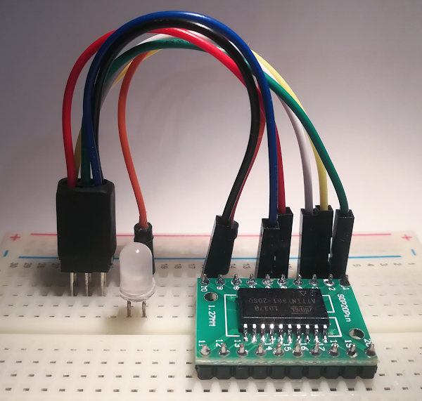
Рис. 2. Макет схемы для программирования микроконтроллера ATtiny861